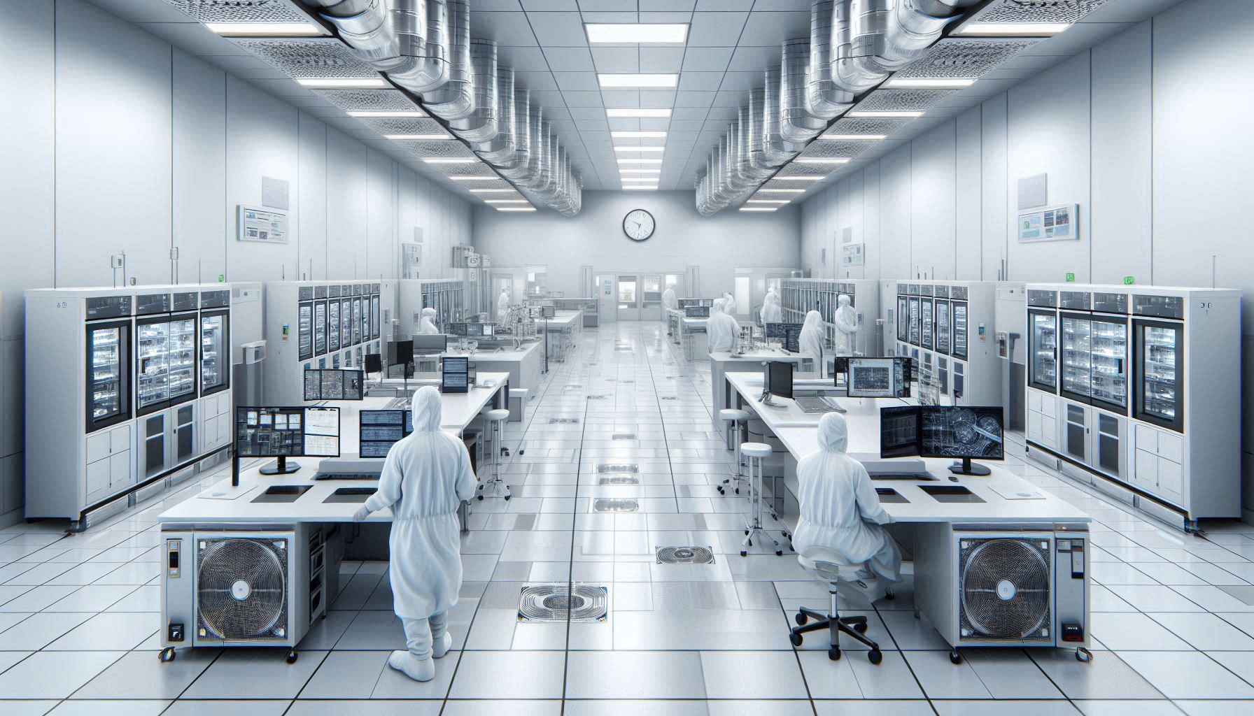
Airborne Contamination Control in Semiconductor Manufacturing is not merely a process; it stands as a cornerstone for ensuring product purity and optimal yield in high-tech production environments. In semiconductor facilities, even the tiniest particle or molecule can have a profound impact on integrated circuit performance. This chapter delves into the critical techniques and strategies that engineers employ to manage and mitigate airborne contaminants. As contamination levels must be controlled down to the submicron scale, the technological approaches outlined here emphasize active monitoring, filtration, and cleanroom design, all essential for maintaining operational excellence in semiconductor manufacturing. In doing so, we explore how effective airborne contamination control directly contributes to enhanced reliability and improved production outcomes.
Understanding Airborne Contamination in Semiconductor Manufacturing
Airborne contamination refers to the presence of undesired particles, chemical vapors, and molecular compounds suspended in the air—elements that can disrupt delicate semiconductor fabrication processes. Within semiconductor manufacturing, such contaminants can originate from construction materials, human activities, and chemical processes. The unique environment of a semiconductor facility requires that every airborne particulate, whether solid or gaseous, be carefully regulated. Engineers and facility managers leverage advanced HVAC systems, coupled with high-efficiency filters, to maintain the stringent cleanliness standards that are paramount for modern chip fabrication. The clarity in understanding these threats fosters the development of innovative contamination control strategies and sophisticated air monitoring systems. For further insights into sophisticated design approaches, one can review our detailed guide on Clean Room Design and Construction.
Sources and Types of Airborne Contaminants in Semiconductor Environments
In semiconductor cleanrooms, airborne contaminants can be broadly categorized into particulate matter, chemical vapors, and microbial agents. Particulates, which include dust and microfibers, are typically generated by human movement, equipment operation, or even from the natural shedding of materials. Chemical vapors—often byproducts of process chemicals—can infiltrate the manufacturing environment, posing risks to delicate circuitry. Furthermore, microbial contaminants, although less common, present potential hazards if proper environmental controls are not in place. Each contaminant type requires specific methods of detection and elimination. Advanced sensors and real-time monitoring systems help detect even trace concentrations, ensuring an immediate response to any deviation from baseline conditions. These vigilant practices enable semiconductor facilities to systematically address potential yield losses.
Impact of Airborne Contamination on Semiconductor Yield and Reliability
The semiconductor industry is extremely sensitive to airborne contamination due to the minuscule dimensions involved in chip fabrication. Even a single microscopic particle can cause defects that compromise the functionality of integrated circuits. Such contaminants can lead to yield losses, increased rework, and even severe operational delays. In many cases, these yield penalties result in significant financial costs and diminished product reliability. It is not uncommon for modern semiconductor fabs to invest heavily in contamination control measures to avoid the devastating impact of so-called “killer defects.” By proactively managing airborne contaminants, manufacturers not only protect their production lines but also foster long-term reliability and performance improvements. This proactive approach ensures that each chip meets the exacting standards dictated by today’s technology nodes.
Filtration Technologies: HEPA and ULPA Filters in Cleanrooms
Filtration technologies are at the heart of airborne contamination control in semiconductor manufacturing. High-Efficiency Particulate Air (HEPA) filters and Ultra-Low Particulate Air (ULPA) filters are engineered to capture extremely small particles, ensuring that only clean air circulates within the production environment. HEPA filters typically remove at least 99.97% of particles down to 0.3 microns, while ULPA filters offer an even higher degree of filtration efficiency. The integration of these filters within HVAC systems designed for semiconductor cleanrooms is critical. In this setting, filter performance is continuously monitored through a combination of differential pressure sensors and periodic validation tests. Such measures guarantee that filters are replaced or serviced before performance degrades, thereby preventing potential contamination events. For instance, a semiconductor facility in India recently reported a 25% reduction in energy use and enhanced yield stability after upgrading its filter system.
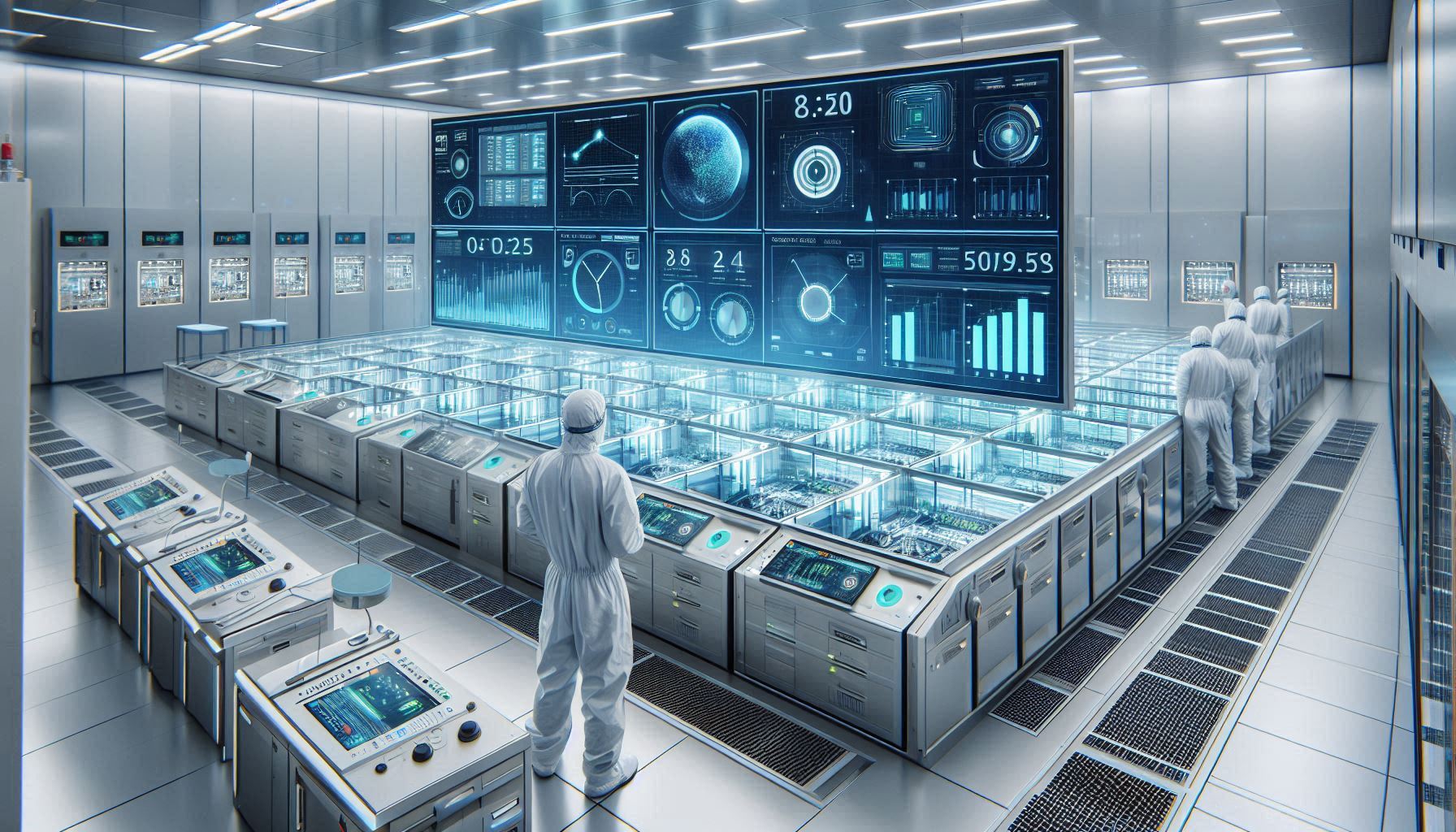
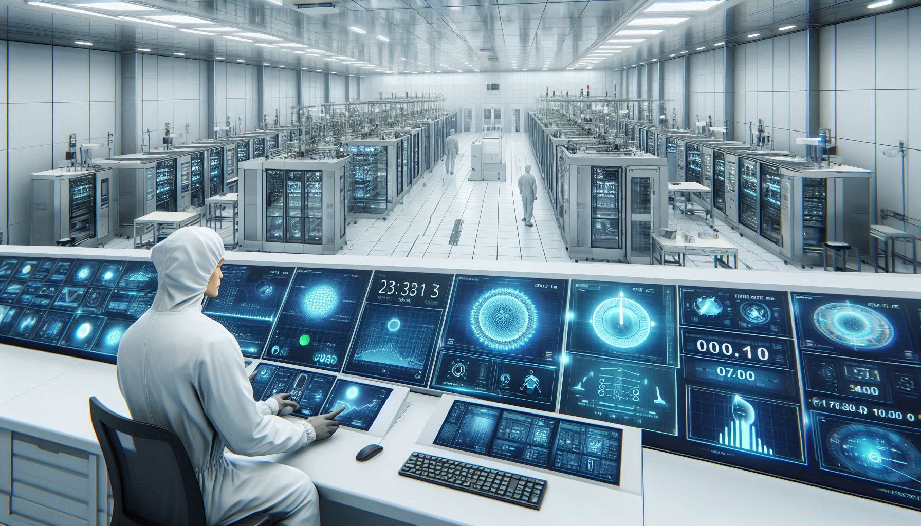
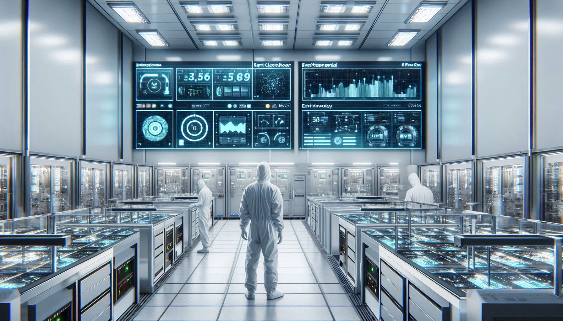
Continuous Monitoring and Real-Time Detection of Airborne Contaminants
Modern semiconductor facilities have embraced continuous monitoring systems that provide real-time insight into airborne contamination levels. Advanced sensors, including ion mobility spectrometers and innovative airborne molecular contaminant detectors, can measure pollutant levels in parts-per-billion (ppb) ranges. These systems are capable of detecting both routine background contaminants and sudden spikes in contamination due to process upsets. By continuously collecting data, facility managers can not only identify emerging issues but also predict trends that may necessitate proactive maintenance or design adjustments. The use of such technology elevates the overall cleanliness and performance of the manufacturing process. In many cases, incorporating smart controllers and automated alerts ensures rapid responses to contamination events, significantly reducing the risk of yield loss. Advanced air quality sensors [like these] also offer affiliate purchasing options that can complement an existing cleanroom setup.
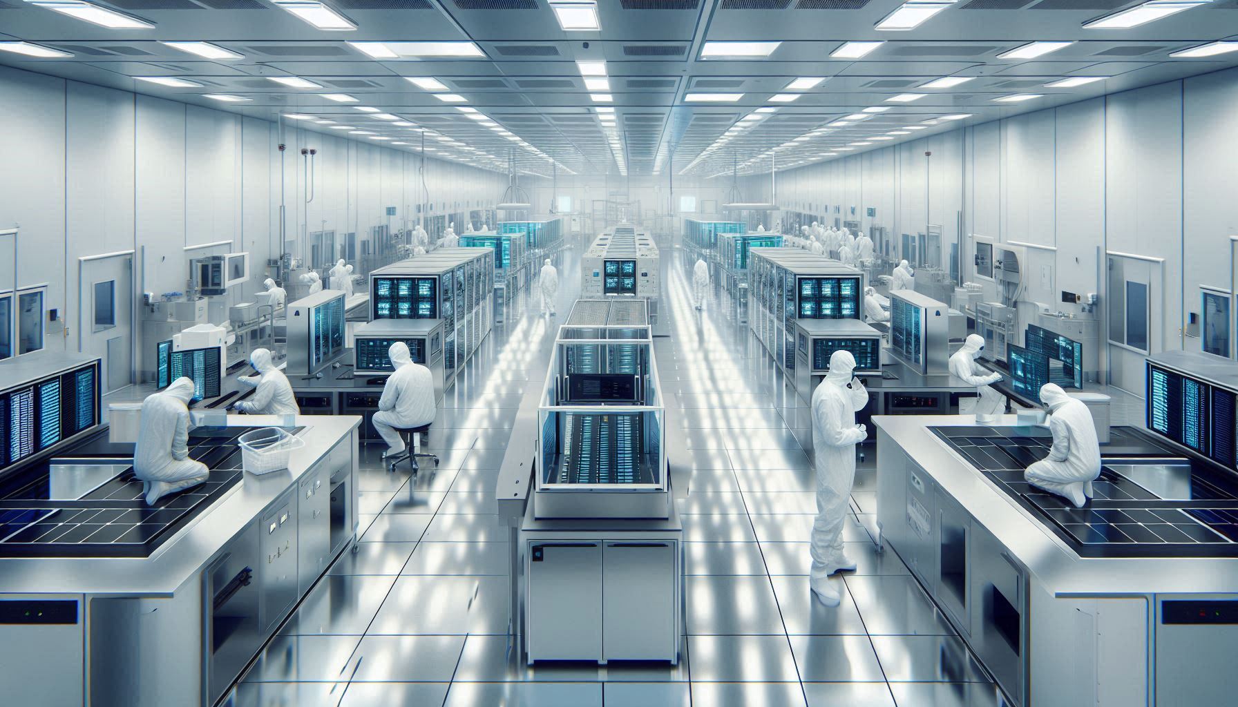
Cleanroom Design for Effective Contamination Control
The blueprint of a semiconductor cleanroom is crucial to the success of its contamination control strategy. Effective design involves strategic layout planning that directs laminar airflow, minimizes turbulence, and segregates critical process areas from potential contamination sources. Careful zoning ensures that personnel, materials, and machinery maintain a disciplined flow throughout the facility. One key aspect is the incorporation of pressure differentials to create gentle barriers between clean and less clean areas. In addition, the design process must consider the integration of advanced HVAC components that support real-time monitoring and rapid environmental adjustments. For detailed methods and innovative strategies in this field, readers may find our article on Cleanroom Design Challenges and How to Overcome Them highly informative. This integrated approach is essential to safeguard the semiconductor manufacturing process against airborne contaminants.
Compliance with International Standards and Codes
Maintaining strict airborne contamination control requires adherence to both national and international standards. Semiconductor facilities in India, for example, must navigate guidelines set by local bodies such as the Bureau of Indian Standards (BIS) in conjunction with globally recognized standards. International codes like ASHRAE and ISHRAE provide rigorous frameworks for HVAC design and operation. Compliance with these standards ensures that cleanroom environments meet necessary criteria for temperature control, humidity regulation, and particulate filtration. Meeting such standards not only boosts process reliability but also reinforces the facility’s commitment to safety and quality. Facility audits and regular performance evaluations serve to validate adherence to these standards and to identify areas for iterative improvement. Overall, global standards push semiconductor manufacturers toward a higher level of operational excellence.
Smart Controls and Automation in Airborne Contamination Control
The rise of digital technologies has revolutionized airborne contamination control in semiconductor manufacturing through the use of smart controls and automation. Intelligent HVAC systems now incorporate machine learning algorithms and IoT connectivity to optimize environmental conditions continuously. Automated systems adjust airflow, pressure, and filtration rates dynamically in response to real-time sensor data. This automation not only enhances precision but also reduces the need for manual intervention, thereby minimizing human error. Smart monitoring solutions enable facility managers to schedule preventive maintenance, predict potential system failures, and quickly respond to any anomaly. Moreover, these systems empower factories to reduce energy consumption while upholding environmental standards. For additional insights on innovative HVAC solutions, check out our article on Innovative HVAC for Semiconductor Manufacturing.
Best Practices and Maintenance Strategies for Contamination Control
Implementing best practices in airborne contamination control involves the coordinated efforts of design, monitoring, and maintenance. Preventive maintenance plays a vital role in ensuring that HVAC systems and associated components like filters and sensors continue to operate at peak performance. Regular cleaning protocols, coupled with re-calibration of monitoring equipment, are essential to detect deviations from the norm. Facilities establish strict gowning and material handling procedures to further minimize the risk of contaminant ingress. Additionally, a culture of continuous improvement drives iterative upgrades, based on performance data trends and technological advances. Detailed documentation and routine training for personnel ensure that everyone in the facility adheres to contamination control protocols. These best practices significantly reduce downtime and maintain high throughput in semiconductor manufacturing.
Case Studies: Successful Implementation in Semiconductor Facilities
Several semiconductor facilities around the world have successfully implemented robust airborne contamination control measures, leading to substantial improvements in yield and efficiency. For example, one facility in Bangalore integrated state-of-the-art real-time monitoring systems with automated filter replacement protocols. This integration not only improved the overall cleanliness of the production environment but also resulted in a significant reduction in maintenance costs. Similarly, a facility in Europe showcased the effectiveness of combining smart controls with advanced HEPA and ULPA filtration, thereby reducing contaminant levels to near-zero. Such case studies highlight the importance of proactive contamination control and serve as benchmarks for other manufacturers. For more on innovative solutions in semiconductor environments, refer to our comprehensive post on India Semiconductor Innovative for Cleanroom Tech for Growth.
Emerging Trends and Future Directions in Contamination Control
The future of airborne contamination control in semiconductor manufacturing appears increasingly intertwined with technological innovation and sustainability. As device geometries become even smaller and production standards more rigorous, emerging trends such as AI-driven analytics, predictive maintenance, and IoT-enabled control systems are set to revolutionize cleanroom operations. Advances in sensor technology, including the use of compact, high-resolution detectors, promise to provide even more granular control of the manufacturing environment. Additionally, sustainable solutions—like energy-efficient HVAC retrofits and green building certifications—are gaining traction. These trends not only pave the way for enhanced contamination control but also align with broader global sustainability goals. Manufacturers who invest in these forward-thinking technologies are well poised to realize significant operational and environmental benefits.
Integrating Advanced Technologies into Existing Systems
Transitioning from traditional contamination control methods to advanced technological solutions can be challenging yet rewarding. Upgrading existing HVAC systems with smart components and enhanced sensors can lead to marked improvements in contamination monitoring and overall air quality management. The integration process usually involves phased implementations and rigorous testing, ensuring that new systems harmonize with legacy infrastructure. Additionally, the integration of advanced data analytics allows facility managers to identify subtle trends in contaminant levels and adjust operations accordingly. This seamless convergence of technology and process management not only maximizes cleanroom performance but also optimizes energy usage and maintenance schedules. Manufacturers have witnessed clear benefits including reduced downtime and improved product quality, thus solidifying the role of modern technologies in airborne contamination control.
The Role of Training and Human Factors
Even in an era of automation, human factors remain critical in the successful control of airborne contamination. Continuous training programs for staff, regular safety drills, and a clear understanding of contamination risks are essential components of a comprehensive control strategy. Personnel are trained to recognize early signs of contamination and to follow strict gowning and procedural protocols. By fostering a culture where every team member is aware of their role in contamination control, semiconductor manufacturers can significantly lower the risk of inadvertent lapses. Moreover, effective communication between technical teams and facility management further enhances response times and preventative measures. The human factor, therefore, acts as both a safeguard and a complement to technological systems, ensuring robust and reliable contamination control.
Operational Challenges and Innovative Solutions
Operating in a semiconductor manufacturing environment is replete with challenges—particularly in managing airborne contaminants. Fluctuating process conditions, unexpected equipment failures, and human error can all contribute to contamination risks. However, innovative engineering solutions are emerging to tackle these obstacles. One notable example is the utilization of real-time analytics powered by AI, which identifies potential contamination events before they escalate. Additionally, modular HVAC designs allow facilities to isolate and address issues rapidly without disrupting the entire cleanroom environment. Such operational innovations not only enhance performance but also boost overall facility resilience. By merging practical experience with cutting-edge technology, semiconductor manufacturers can effectively maintain stringent airborne contamination control.
Maintaining a Competitive Edge through Airborne Contamination Control
In today’s tough semiconductor market, keeping a clean manufacturing environment is key to success. Proactive airborne contamination control translates into improved yield, reduced rework costs, and enhanced product reliability. Businesses that prioritize these measures position themselves at the forefront of technological innovation, ensuring that they can meet the ever-evolving demands of a high-tech market. Ultimately, efficient contamination control instills confidence in clients and stakeholders alike. It becomes a strategic asset, driving operational excellence and strengthening a company’s competitive advantage. As the industry continues to evolve, those who invest in robust control systems will likely achieve sustained success in both performance and profitability.
FAQs
1. What are the primary sources of airborne contamination in semiconductor manufacturing?
Airborne contaminants can arise from human movement, process chemicals, construction materials, and even equipment operation. Dust, chemical vapors, and microbial agents can negatively impact production quality, making rigorous air filtration and control essential.
2. How do HEPA and ULPA filters contribute to contamination control?
HEPA filters capture 99.97% of particles down to 0.3 microns, and ULPA filters provide even better filtration. These filters ensure clean air circulation, preventing microscopic particles from affecting semiconductor fabrication processes.
3. Why is airborne contamination a critical concern in semiconductor fabrication?
Semiconductor chips are highly sensitive to even the smallest impurities. Airborne particles can lead to defects in microcircuits, causing yield losses and reliability issues in finished products.
4. How does HVAC design impact contamination control in semiconductor cleanrooms?
Proper HVAC systems regulate airflow, maintain temperature and humidity stability, and utilize pressure differentials to prevent contaminants from migrating into critical areas. Smart monitoring further enhances control.
5. What role do advanced air monitoring systems play in contamination prevention?
Real-time monitoring sensors detect airborne contaminants at submicron levels, enabling immediate adjustments in air filtration and airflow. These systems help minimize contamination risks and maintain stringent cleanliness standards.
6. How do cleanroom zoning strategies help minimize contamination?
Cleanroom zoning involves segmenting areas based on contamination sensitivity. Pressure differentials between zones prevent cross-contamination, ensuring a controlled environment where airborne particles are kept at bay.
7. What international standards govern airborne contamination control in semiconductor facilities?
Semiconductor cleanrooms follow global standards like ISO 14644, ASHRAE, and ISHRAE for air quality, HVAC systems, and contamination control practices.
8. What are the future trends in airborne contamination control for semiconductor manufacturing?
AI-driven analytics, IoT-enabled sensors, and real-time predictive maintenance are shaping contamination control strategies. Sustainable filtration solutions and automated airflow adjustments further optimize cleanroom conditions.
About the Author
Mr. Om Prakash, with over 18 years of hands-on experience in the HVAC industry, brings unmatched expertise in cleanroom, pharmaceutical, semiconductor, data center, commercial, and industrial HVAC systems. As the founder of HVAC Technocrat, he specializes in customized HVAC design, energy efficiency audits, retrofit planning, and turnkey consultancy services across India. His deep understanding of critical environments and complex building needs ensures every solution is efficient, reliable, and future-ready. Through his writings, he simplifies HVAC concepts and shares real-world insights to support professionals, facility managers, and decision-makers. For any enquiries or project support, feel free to call or WhatsApp at +91 9908091942, email at hvactechnocrats@gmail.com, or visit www.hvactechnocrat.com also follow LinkedIn profile: https://www.linkedin.com/in/hvactechnocrats/
Disclaimer:
The content here is intended solely for educational and informational purposes. All case studies, examples, and hypothetical scenarios are illustrative in nature and do not refer to, endorse, or represent any actual company, organization, or product. Any similarity to real-world entities or events is purely coincidental. Readers are encouraged to verify any technical details or operational recommendations with additional, independent research prior to implementation. The author and publisher assume no responsibility or liability for any errors, omissions, or outcomes resulting from the use of this material.