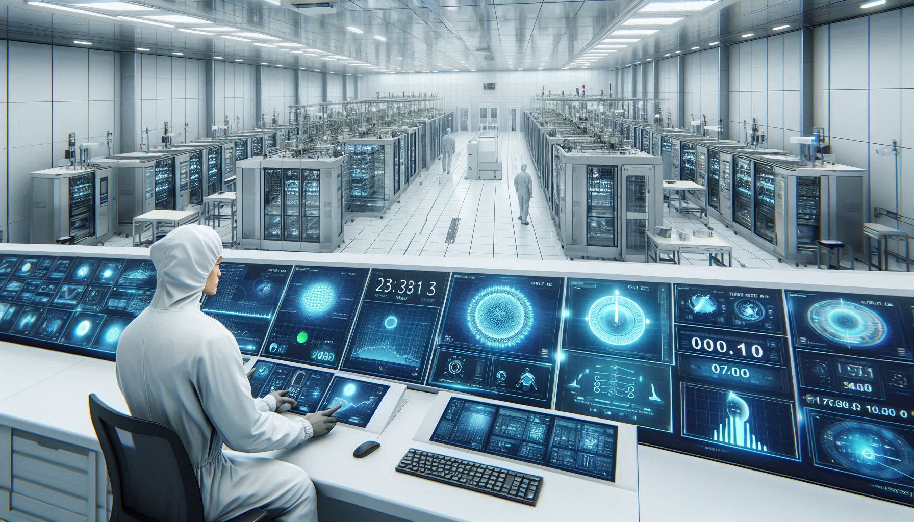
Semiconductor Cleanroom Zoning: Best Practices of contamination control

Semiconductor Cleanroom Zoning layout in a semiconductor manufacturing facility to control contamination.

Semiconductor cleanroom zoning represents the backbone of contamination control in modern chip manufacturing facilities. This systematic approach to space planning ensures that different manufacturing processes operate within their required cleanliness levels while preventing cross-contamination between zones. The concept extends far beyond simple room separation, incorporating sophisticated airflow management, pressure differentials, and material flow control mechanisms that collectively maintain the sterile environment essential for semiconductor production.

Understanding the Critical Role of Semiconductor Cleanroom Zoning

The importance of proper zoning becomes evident when considering that a single particle measuring just 0.1 micrometers can destroy an entire semiconductor wafer worth thousands of dollars. Indian semiconductor facilities, particularly those emerging under government initiatives like the Production Linked Incentive scheme, must implement robust zoning strategies to compete globally. These facilities typically handle everything from basic assembly operations to advanced wafer fabrication, each requiring distinct contamination control approaches that reflect international standards while adapting to local operational conditions.

Effective zoning strategies directly impact production yield, operational efficiency, and compliance with international standards such as ISO 14644-1 and various semiconductor industry specifications. The complexity increases when facilities must accommodate multiple product lines, different cleanliness requirements, and varying process technologies within a single building envelope. Understanding these fundamentals forms the foundation for developing comprehensive contamination control strategies.

Enjoying this content? Get expert HVAC updates on our Telegram Channel.

Wafer Fab Layout Optimization Through Strategic Zone Planning

Wafer fab layout optimization demands careful consideration of process flow, equipment placement, and personnel movement patterns to minimize contamination risks. The traditional approach involves creating a linear flow from raw wafer input through various processing steps to final testing and packaging. However, modern facilities often require more complex layouts that accommodate multiple process lines, shared utilities, and flexible manufacturing capabilities while maintaining strict contamination control.

The optimization process begins with mapping critical process steps and identifying contamination-sensitive operations. Photolithography areas typically require the highest cleanliness levels, often ISO Class 1 or Class 10, while mechanical assembly operations might function adequately in Class 1000 or Class 10000 environments. This hierarchy drives the overall facility layout, with the cleanest areas positioned at the facility core and progressively less critical zones arranged in concentric rings around this central clean zone.

Modern Indian semiconductor facilities increasingly adopt the ballroom concept, where large open cleanroom spaces house multiple process tools with flexible reconfiguration capabilities. This approach offers significant advantages in terms of airflow management, equipment access, and future expansion possibilities. The ballroom layout typically features a raised floor system for utilities distribution and a sophisticated ceiling-mounted air handling system that provides laminar airflow across the entire space.

Personnel and material flow patterns significantly influence layout optimization decisions. Successful designs incorporate separate pathways for people and materials, with dedicated airlocks, gowning areas, and decontamination stations positioned strategically throughout the facility. The goal involves minimizing travel distances while ensuring that all movements follow contamination control protocols. Advanced facilities implement automated material handling systems that further reduce human presence in the most critical zones.

Chip Manufacturing Area Segregation Principles

Chip manufacturing area segregation operates on the fundamental principle that different manufacturing processes generate varying types and levels of contamination. Wet chemical processes, plasma etching, ion implantation, and photolithography each present unique challenges that require specific containment and isolation strategies. Effective segregation ensures that contamination from one process does not compromise the cleanliness requirements of adjacent operations.

Chemical segregation represents one of the most critical aspects of area planning in semiconductor facilities. Wet benches handling hydrofluoric acid require specialized exhaust systems and corrosion-resistant materials, while organic solvent processes demand explosion-proof electrical systems and appropriate fire suppression measures. These chemical-specific requirements often drive the decision to create dedicated zones with their own air handling systems, preventing cross-contamination between incompatible processes.

Particle generation characteristics also influence segregation decisions. Mechanical processes such as wafer dicing, grinding, and packaging operations generate significantly more particles than chemical vapor deposition or photolithography processes. Facilities typically locate high-particle-generation processes in separate zones with enhanced air filtration and higher air change rates to contain contamination at its source.

Temperature and humidity requirements further complicate segregation planning. Photolithography processes often require precise temperature control within ±0.1°C, while furnace operations might tolerate broader temperature ranges. Humidity sensitivity varies dramatically between processes, with some requiring less than 1% relative humidity while others function adequately at standard cleanroom conditions of 45±5% RH. These environmental requirements often necessitate separate air handling systems for different zones.

Cleanroom Classification Zones and Compliance Requirements

Cleanroom classification zones must align with specific industry standards and product requirements while providing practical operational flexibility. The ISO 14644-1 standard provides the international framework for cleanroom classification, defining particle concentration limits for different cleanliness classes. Indian semiconductor facilities typically implement multiple classification zones within a single facility, ranging from ISO Class 1 for critical photolithography areas to ISO Class 8 for packaging and assembly operations.

The classification system considers both particle size and concentration, with measurements typically conducted using laser particle counters capable of detecting particles as small as 0.1 micrometers. Class 1 cleanrooms permit no more than 10 particles per cubic meter of 0.1-micrometer size, while Class 100 allows up to 3,520 particles of the same size per cubic meter. These stringent requirements demand sophisticated air filtration systems, typically employing HEPA or ULPA filters with 99.999% efficiency ratings.

Monitoring and verification requirements add another layer of complexity to classification zone management. Facilities must conduct regular particle counts, airflow measurements, and filter integrity tests to maintain certification. Indian facilities often face additional challenges related to external environmental conditions, including higher dust levels and seasonal variations that can impact cleanroom performance. Successful operations implement continuous monitoring systems that provide real-time data on particle levels, allowing for immediate corrective actions when deviations occur.

The transition zones between different classification areas require careful design attention to prevent contamination migration. These areas typically incorporate air locks, pressure cascades, and specialized air handling systems that maintain appropriate pressure differentials while allowing personnel and material movement. The pressure differential between adjacent zones should typically maintain at least 2.5 Pascals, with higher differentials used when significant cleanliness differences exist.

Fab Facility Space Planning for Optimal Contamination Control

Fab facility space planning integrates multiple engineering disciplines to create environments that support both current operations and future expansion needs. The planning process must consider structural requirements, utility distribution, equipment access, emergency egress, and contamination control measures within a cohesive design framework. Modern facilities typically allocate 60-70% of total floor area to production spaces, with the remainder dedicated to support functions including mechanical rooms, offices, and material storage areas.

The vertical organization of fab facilities significantly impacts contamination control effectiveness. Most facilities employ a three-level design with mechanical equipment located on the top floor, cleanroom production areas on the middle level, and utility distribution through a raised floor system at the bottom level. This arrangement facilitates gravity-fed exhaust systems, simplified utility routing, and effective separation of clean and potentially contaminated zones.

Utility distribution planning requires careful coordination to minimize contamination risks while providing necessary services to all areas. Chemical distribution systems typically utilize dedicated corridors or interstitial spaces to isolate potentially hazardous materials from production areas. Electrical systems must comply with explosion-proof requirements in certain zones while providing the clean, stable power required for sensitive semiconductor equipment.

Future flexibility considerations increasingly influence space planning decisions as semiconductor technology continues evolving rapidly. Facilities must accommodate equipment changes, process modifications, and capacity expansions without compromising contamination control integrity. This requirement often drives decisions toward larger open spaces with flexible utility connections rather than fixed, process-specific room layouts.

Advanced Airflow Management Systems in Zoned Environments

Advanced airflow management systems form the technical foundation of effective cleanroom zoning, providing the means to maintain required particle levels while accommodating complex facility layouts. These systems must deliver appropriate air volumes, maintain pressure differentials, provide uniform air distribution, and minimize energy consumption across multiple zones with varying requirements. Modern facilities typically employ computer-based airflow simulation during design phases to optimize system performance and identify potential problem areas.

Laminar airflow systems represent the gold standard for critical semiconductor processes, providing unidirectional airflow that sweeps particles away from sensitive areas. These systems typically operate at velocities between 0.3 and 0.5 meters per second, creating a laminar boundary layer that prevents turbulent mixing and particle recirculation. The implementation requires precision-engineered air distribution systems with HEPA or ULPA filtration, often consuming 30-40% of total facility energy.

Mixed airflow systems offer energy advantages in less critical areas while maintaining adequate contamination control. These systems combine high-efficiency filtration with strategic air distribution to achieve required particle levels at lower energy costs. The key involves understanding particle generation patterns and designing airflow systems that capture contamination at its source before it can spread throughout the space.

Pressure cascade management becomes critical when multiple zones with different cleanliness requirements connect within a single facility. The system must maintain appropriate pressure differentials across all boundaries while accommodating door openings, equipment installations, and normal operational activities. Advanced facilities implement automated pressure control systems that adjust airflow rates in real-time to maintain required differentials despite changing conditions.

Contamination Source Identification and Control Strategies

Contamination source identification requires systematic analysis of all potential particle and chemical sources within semiconductor facilities. Human activities typically represent the largest contamination source, with personnel generating particles through skin shedding, clothing fibers, and respiratory emissions. Equipment operations contribute mechanical particles, chemical residues, and electromagnetic interference that can impact sensitive processes. External sources including outdoor air, construction activities, and utility systems add additional contamination challenges.

Personnel contamination control strategies encompass comprehensive gowning procedures, training programs, and behavioral modifications designed to minimize particle generation. Modern facilities implement multi-stage gowning sequences with air showers, sticky mats, and ionization systems that remove particles and static charges before personnel enter critical areas. The effectiveness depends heavily on employee training and adherence to established procedures, making ongoing education programs essential for maintaining contamination control standards.

Equipment-related contamination control focuses on both source elimination and containment strategies. Preventive maintenance programs help minimize particle generation from mechanical wear, while specialized enclosures contain contamination from high-particle-generation processes. Advanced facilities implement real-time particle monitoring systems that automatically adjust air filtration rates when equipment-generated contamination exceeds predetermined thresholds.

Chemical contamination presents unique challenges requiring specialized detection and control strategies. Outgassing from construction materials, cleaning solvents, and process chemicals can create molecular contamination that interferes with semiconductor processes even at extremely low concentrations. Facilities typically implement material selection programs, bake-out procedures, and specialized filtration systems designed to remove molecular contaminants from the cleanroom environment.

Environmental Control Integration Across Multiple Zones

Environmental control integration demands sophisticated coordination between temperature, humidity, pressure, and air quality management systems across multiple zones with varying requirements. The complexity increases when facilities must accommodate incompatible environmental conditions within adjacent spaces while maintaining energy efficiency and operational flexibility. Modern systems typically employ computer-based control strategies that optimize performance across all zones simultaneously rather than treating each area independently.

Temperature control strategies must address both sensible and latent heat loads while maintaining the precision required for semiconductor processes. Critical photolithography areas often require temperature stability within ±0.1°C, while general manufacturing areas might tolerate ±1°C variations. The challenge involves designing systems that provide required precision in critical areas without overconditioning less sensitive zones, which would waste energy and create operational inefficiencies.

Humidity control becomes particularly challenging in facilities with multiple zones requiring different moisture levels. Photolithography processes typically require very low humidity levels to prevent resist adhesion problems, while some chemical processes function better at moderate humidity levels that reduce static electricity generation. The solution often involves dedicated air handling systems for each zone with different humidity requirements, coupled with sophisticated moisture management strategies.

Integration challenges extend beyond basic environmental parameters to include air quality management, pressure control, and emergency response capabilities. Systems must coordinate responses to equipment failures, power outages, and other emergency conditions while maintaining contamination control integrity. Advanced facilities implement redundant systems and fail-safe operating modes that ensure critical areas remain protected even during equipment failures or maintenance activities.

Technology Integration for Smart Cleanroom Operations

Technology integration transforms traditional cleanroom operations through automation, real-time monitoring, and predictive maintenance capabilities that enhance contamination control effectiveness while reducing operational costs. Modern facilities typically implement integrated building management systems that coordinate HVAC operations, particle monitoring, access control, and emergency response functions through centralized control platforms. These systems provide operators with comprehensive facility status information and automated responses to changing conditions.

Sensor networks enable continuous monitoring of critical parameters including particle levels, temperature, humidity, pressure differentials, and chemical concentrations throughout the facility. Advanced systems employ wireless sensor networks that eliminate potential contamination sources associated with traditional wiring while providing flexible monitoring capabilities that can adapt to changing facility layouts. The data collected supports both real-time operational decisions and long-term performance optimization strategies.

Artificial intelligence applications increasingly support cleanroom operations through predictive maintenance programs, energy optimization algorithms, and contamination source identification systems. Machine learning algorithms analyze historical performance data to identify patterns that predict equipment failures, optimize filter replacement schedules, and recommend operational adjustments that improve contamination control effectiveness. These capabilities become particularly valuable in large facilities with complex interconnected systems.

Digital twin technology represents the latest advancement in cleanroom management, creating virtual facility models that support operational optimization, staff training, and scenario planning activities. These models incorporate real-time sensor data, equipment performance information, and environmental conditions to provide accurate representations of facility operations. Operators can use digital twins to test operational changes, train personnel, and optimize system performance without impacting actual production operations.

Energy Efficiency Considerations in Multi-Zone Design

Energy efficiency considerations significantly impact the economic viability of semiconductor cleanroom operations, with HVAC systems typically consuming 40-60% of total facility energy. Multi-zone designs offer opportunities for optimization through load matching, equipment right-sizing, and operational scheduling strategies that reduce energy consumption while maintaining required environmental conditions. The key involves understanding the relationship between contamination control requirements and energy consumption to identify optimization opportunities.

Heat recovery systems provide significant energy savings opportunities in facilities with simultaneous heating and cooling requirements. Many semiconductor processes generate substantial heat loads that must be removed from cleanroom areas, while other areas require heating during certain operational periods. Heat recovery systems capture waste heat from exhaust airstreams and use it to condition incoming fresh air, reducing both heating and cooling energy requirements.

Variable air volume systems enable energy optimization by adjusting airflow rates based on actual contamination control requirements rather than maintaining constant maximum flow rates. These systems typically incorporate real-time particle monitoring that automatically adjusts air change rates when contamination levels change. During periods of reduced activity, such as overnight or weekend operations, airflow rates can be reduced significantly while maintaining required cleanliness levels.

Equipment optimization strategies focus on improving the efficiency of individual system components including fans, pumps, chillers, and air handling units. Modern facilities typically employ high-efficiency equipment with variable speed drives that adjust operating parameters based on actual load requirements. Regular maintenance programs ensure equipment operates at peak efficiency, while equipment replacement programs systematically upgrade older, less efficient components.

Regulatory Compliance and Industry Standards

Regulatory compliance requirements significantly influence cleanroom zoning decisions, with facilities must meeting various national and international standards depending on their products and markets. Indian semiconductor facilities typically must comply with BIS standards, ISHRAE guidelines, international ISO standards, and specific customer requirements that may impose additional restrictions. The complexity increases when facilities serve multiple markets with different regulatory requirements.

ISO 14644-1 provides the primary international framework for cleanroom classification and testing procedures. This standard defines particle concentration limits for different cleanliness classes while specifying testing methods, monitoring frequencies, and certification requirements. Facilities must demonstrate compliance through regular testing programs that document particle levels, airflow rates, and filter performance across all classified areas.

ASHRAE standards provide guidance on HVAC system design, operation, and maintenance practices that support cleanroom applications. These standards address air filtration requirements, energy efficiency considerations, and indoor air quality management strategies that complement ISO cleanroom standards. The integration of multiple standards requires careful coordination to ensure all requirements are met without creating conflicting operational constraints.

Industry-specific standards add another layer of complexity, with semiconductor manufacturers often imposing requirements that exceed general cleanroom standards. These specifications typically address specific contamination concerns related to particular manufacturing processes, materials compatibility requirements, and quality assurance procedures that support high-yield production operations. Facilities serving multiple customers may need to accommodate different standards simultaneously within the same building.

Future Trends and Emerging Technologies

Future trends in semiconductor cleanroom zoning reflect ongoing advances in manufacturing technology, environmental control systems, and automation capabilities that promise to improve contamination control effectiveness while reducing operational costs. The industry continues moving toward smaller feature sizes and more complex manufacturing processes that demand increasingly sophisticated contamination control strategies. These trends drive innovations in facility design, equipment technology, and operational procedures.

Nanotechnology applications are emerging in air filtration systems, offering improved particle removal efficiency and lower pressure drops compared to traditional HEPA and ULPA filters. These advanced filtration media employ nanofiber technology that creates smaller pore sizes while maintaining high airflow rates. The technology promises significant energy savings while providing superior contamination control performance.

Advanced monitoring technologies including real-time molecular contamination detection, automated particle sizing, and wireless sensor networks provide unprecedented visibility into cleanroom performance. These systems enable proactive contamination control strategies that identify and address problems before they impact production operations. The integration with artificial intelligence algorithms supports predictive maintenance programs and operational optimization strategies that improve overall facility performance.

Sustainable design principles increasingly influence cleanroom development, with facilities incorporating renewable energy systems, water recycling programs, and waste minimization strategies that reduce environmental impact while maintaining required performance levels. These approaches align with corporate sustainability goals while potentially reducing operational costs through resource conservation and efficiency improvements.

Frequently Asked Questions

How to control contamination in a clean room?

Contamination control in cleanrooms requires a comprehensive approach combining advanced air filtration, positive pressure maintenance, strict personnel protocols, and regular monitoring. The primary strategy involves creating laminar airflow patterns that continuously remove particles while preventing external contamination entry through pressure cascades and airlocks.

What does class 100 and class 1000 clean room mean?

Class 100 cleanrooms allow maximum 100 particles of 0.5 micrometers per cubic foot, equivalent to ISO Class 5. Class 1000 permits up to 1000 particles of the same size, corresponding to ISO Class 6. These classifications define the maximum allowable particle concentrations for different manufacturing processes.

What are the clean room standards for semiconductors?

Semiconductor cleanroom standards primarily follow ISO 14644-1 for classification, with specific areas requiring ISO Class 1-5 depending on process sensitivity. Additional standards include SEMI specifications for equipment, ASHRAE guidelines for HVAC systems, and industry-specific requirements for molecular contamination control and electrostatic discharge protection.

How does a cleanroom primarily prevent contamination?

Cleanrooms prevent contamination through engineered airflow systems that create positive pressure environments with continuous air filtration. HEPA or ULPA filters remove particles while laminar airflow patterns sweep contaminants away from sensitive areas. Personnel protocols and material control procedures minimize contamination introduction.

What is the clean room market for semiconductors?

The global semiconductor cleanroom market is experiencing rapid growth, particularly in Asia-Pacific regions including India. Market expansion is driven by increasing semiconductor demand, advanced manufacturing technologies, and government initiatives supporting domestic chip production. The market encompasses construction, equipment, and ongoing operational services.

What are the key factors in cleanroom zone design?

Key factors include process compatibility, contamination sensitivity levels, personnel and material flow patterns, utility requirements, regulatory compliance needs, and future flexibility requirements. Successful designs integrate these factors while optimizing energy efficiency and operational costs throughout the facility lifecycle.

Disclaimer

The content here is intended solely for educational and informational purposes. All case studies, examples, and hypothetical scenarios are illustrative in nature and do not refer to, endorse, or represent any actual company, organization, or product. Any similarity to real-world entities or events is purely coincidental. Readers are encouraged to verify any technical details or operational recommendations with additional, independent research prior to implementation. The author and publisher assume no responsibility or liability for any errors, omissions, or outcomes resulting from the use of this material.

About the Author

Mr. Om Prakash, with over 18 years of hands-on experience in the HVAC industry, brings unmatched expertise in cleanroom, semiconductor, pharmaceutical, data center, commercial, and industrial HVAC systems. As the founder of HVAC Technocrat, he specializes in customized HVAC design, energy efficiency audits, retrofit planning, and turnkey consultancy services across India. He simplifies complex HVAC concepts and shares real-world insights to support professionals, facility managers, and decision-makers. For enquiries or project support, call or WhatsApp at +91 9908091942, email hvactechnocrats@gmail.com, or visit www.hvactechnocrat.com. Also, follow his LinkedIn profile.

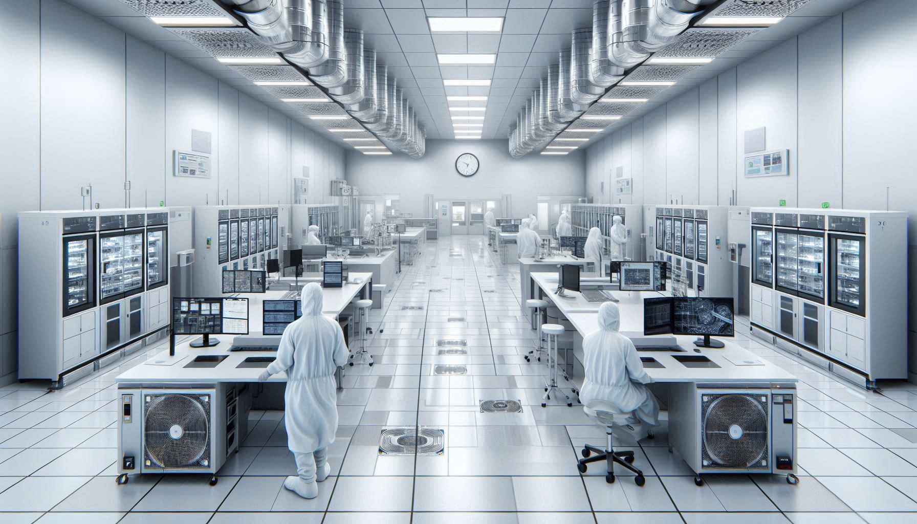
How to Calculate Semiconductor ACPH and Airflow

Advanced semiconductor ACPH clean room with HVAC system showcasing ACH and airflow management

Semiconductor clean rooms demand precise environmental control. In these facilities, engineers design HVAC systems that calculate air changes per hour ACPH and manage airflow requirements with extreme accuracy. Semiconductor clean room performance depends on proper ACPH calculations, as even small errors may affect wafer quality and chip performance. In semiconductor manufacturing, ensuring that HEPA filtration, temperature regulation, and humidity control work harmoniously is critical. This article explains how to calculate semiconductor ACPH, determine proper airflow, and implement effective HVAC designs for semiconductor clean rooms.

Understanding the Concept of Semiconductor ACPH in Clean Rooms

Air changes per hour (ACPH) represent the number of times a room’s air volume is completely exchanged in one hour. In semiconductor clean rooms, engineers calculate ACH by dividing the total volume of air supplied by the room volume. Practically, designers measure the airflow in cubic meters per hour and divide it by the clean room’s volume in cubic meters. ACH plays a key role in controlling airborne contaminants and ensuring the clean room maintains its designated classification. For example, excessive airflow may lower energy efficiency, whereas insufficient airflow can lead to contamination. Therefore, the balance achieved through accurate ACH calculations supports continuous production stability and robust contamination control.

Furthermore, semiconductor clean room ACH calculations help designers determine the optimum layout of fan filter units (FFUs) and ductwork. An optimized ACH ensures that ultra-clean air flows uniformly over sensitive equipment. Manufacturers also use computer-based airflow simulations to verify that calculated ACH meets real-world performance. Industry standards such as ISO 14644-1 and guidelines from ASHRAE and ISHRAE ensure that semiconductor facilities conform to regulatory requirements. Properly calculated ACH reduces the probability of airborne contaminants interfering with chip manufacturing processes.

Calculating Semiconductor ACPH and Airflow Requirements in Clean Rooms

Engineers determine airflow by considering clean room dimensions, occupancy, equipment heat loads, and contamination risks. Designers calculate required air volume by multiplying air changes per hour (ACH) with the room’s volume. Typically, clean room airflow is measured in cubic meters per hour (m³/h) or cubic feet per minute (CFM). For semiconductor applications, airflow must maintain a unidirectional (laminar) pattern that pushes contaminants away from production areas.

Additionally, advanced HVAC systems monitor airflow rates continuously. They adjust fan speeds and duct configurations, thereby ensuring that the volume of air delivered meets exact process requirements. Semiconductor clean room designs include sensors that track air velocity and supply volumes, providing instant feedback if deviations occur. This proactive approach helps minimize downtime and ensures that even minor fluctuations in airflow do not compromise the manufacturing environment.

Key HVAC Parameters and Their Importance in Semiconductor Clean Rooms

Several HVAC parameters influence semiconductor clean room performance. Besides ACH, engineers carefully control temperature, humidity, and positive pressure. Temperature stability within a range of 20°C to 22°C (±0.1°C) prevents thermal expansion or contraction that may cause defects during photolithography. Humidity control (typically maintained between 40% and 60% relative humidity) reduces the risk of electrostatic discharge (ESD) and condensation issues. Positive pressure in the cleanroom prevents unfiltered air from entering from surrounding areas.

Moreover, designers plan the placement of supply diffusers and return vents to achieve uniform airflow distribution. Proper pressure gradients and airflow zoning guarantee that contaminants do not settle on critical wafers. Integrating smart controls into HVAC systems further refines the operation by automatically adjusting to changes in environmental conditions. These measures not only protect semiconductor products but can also lead to energy savings and reduced operational costs.

Methods and Formulas for Calculating Semiconductor ACPH Clean Rooms

Calculating ACH follows a simple formula:

ACH = (Airflow Rate ÷ Room Volume)

For example, if a clean room has a volume of 1,000 m³, and the HVAC system delivers 20,000 m³/h, then:

ACPH = 20,000 ÷ 1,000 = 20 air changes per hour

Q = Volume x ACPH / 60; where Q in cubic feet per min, Volume in cubit feet, ACPH in number

Additionally, engineers often convert airflow from CFM to m³/h (1 CFM ≈ 1.7 m³/h) and consider these conversions during design calculations. Furthermore, designers factor in the efficiency of ductwork and filter media, which might lower the effective airflow delivered.

Case studies reveal that semiconductor facilities in India have achieved optimized ACH by carefully balancing airflow with energy considerations. In one anonymized case study, a semiconductor plant improved its yield by 15% after recalculating ACH to better match clean room dimensions and process requirements. This demonstrates that precise measurement and control of ACH directly impact production efficiency.

Airflow Measurement Techniques and Instrumentation

Accurate airflow measurement is pivotal for proper ACH calculations. Engineers use an array of instruments, such as anemometers, airflow capture hoods, and manometers. These devices provide real-time measurements of air velocity and pressure. For instance, digital anemometers measure the speed of the air flowing out of fan filter units, which is then used in the ACH formula.

Moreover, sensors in the HVAC system alert operators if airflow falls below required levels. Continuous monitoring not only helps maintain clean room classification but also supports energy-efficient operation. A semiconductor clean room with misaligned airflow may experience increased energy consumption or, worse, contamination issues. Utilizing modern instrumentation thus ensures that semiconductor HVAC systems perform reliably over time.

Optimizing HVAC System Design for Semiconductor Clean Rooms

Optimal HVAC system design for semiconductor clean rooms includes several aspects:

  • Precise Calculations: Use accurate measurements for ACH and total airflow, ensuring uniform distribution.
  • Efficient Filtration: Integrate HEPA filters with a high removal efficiency (99.97% at 0.3 microns), which maintain low particle counts.
  • Smart Controls: Implement sensor networks and building automation systems (BAS) that adjust air supply dynamically.
  • Energy Efficiency: Design systems that balance high airflow with low energy consumption by using variable frequency drives (VFDs) and heat recovery measures.

Designers also use computer-based simulations to model airflow trajectories. This method, known as CFD (computer-based airflow simulations), helps predict how air moves throughout the clean room. Internal links to detailed guides on Clean Room Design and Construction provide more insights on this topic. Such simulations contribute to achieving the optimal balance between contamination control and energy efficiency.

Impact of Room Layout and Geometry on Airflow Requirements

Room layout and geometry significantly affect airflow performance. Semiconductor clean rooms use a combination of modular panels, raised floors, and dedicated gowning zones to optimize airflow. The placement of equipment, workstations, and staff affects how clean air flows throughout the room. Engineers design layouts that support unidirectional airflow, which clears out contaminants quickly and prevents stagnation.

For example, facilities in semiconductor manufacturing incorporate zigzag or serpentine airflow patterns to avoid dead zones. Additionally, strategic placement of diffusers ensures that air reaches every part of the clean room. These design choices not only improve the effectiveness of HVAC systems but also enhance energy efficiency by minimizing the need for excessive airflow.

Challenges in Calculating Ach and Airflow in Semiconductor Clean Rooms

Several challenges arise when calculating ACH and airflow in semiconductor clean rooms. First, the complex geometry of high-density equipment and varying occupancy levels can lead to uneven air distribution. Second, filters and ducts may introduce pressure drops, which affect the actual airflow rate delivered to the clean room space. Third, the dynamic nature of manufacturing processes means that airflow requirements may change over time.

Engineers must address these issues by performing regular audits, conducting CFD analyses, and recalibrating sensors. In one case study from India, recalibration of airflow systems led to a 10% energy savings and a more uniform ACH across production areas. By overcoming these challenges, semiconductor facilities improve both product yield and operational cost-effectiveness.

Future Trends: AI, IoT, and Smart Monitoring in ACH Calculations

Emerging technologies such as artificial intelligence (AI) and the Internet of Things (IoT) are revolutionizing HVAC system optimization. Modern semiconductor clean rooms now utilize smart sensors that continuously feed data about temperature, humidity, and airflow into centralized control systems. AI algorithms analyze these data streams in real time, predicting maintenance needs and optimizing air delivery for the calculated ACH.

For example, early AI-driven predictive analytics have helped reduce downtime by alerting facility operators to potential system inefficiencies before they cause contamination events. IoT connectivity further supports energy-efficient operations by automatically adjusting fan speeds and air distribution based on process demands. These innovations promise greater precision in ACH calculations and a more sustainable operation.

Calculating ACH: Practical Case Studies and Industry Examples

Several semiconductor clean room facilities have successfully optimized their HVAC systems by closely monitoring ACH. One semiconductor plant in Hyderabad recalculated its airflow requirements by installing advanced sensors and integrating a smart BAS. This resulted in a 15% increase in yield and a 10% decrease in energy costs. Another example from a facility in South Korea demonstrated that recalculating ACH to account for recirculating air improved contamination control and extended filter lifespan.

These case studies underscore how crucial accurate ACH calculations are in real-world scenarios. They offer practical insights into how minor adjustments in airflow rates can yield significant benefits in terms of performance and cost savings.

Strategies for Enhancing Energy Efficiency and Airflow Control

Semiconductor clean room HVAC systems must balance high performance with energy efficiency. Several strategies help achieve this balance:

  • Variable Frequency Drives (VFDs): Adjust fan speeds automatically based on real-time process requirements.
  • Heat Recovery Systems: Reuse waste heat from the clean room to pre-condition incoming air.
  • Regular Maintenance and Calibration: Maintain sensor accuracy and system performance to ensure that calculated ACH remains reliable over time.
  • Design Optimization: Use CFD simulations to optimize duct routes and diffusers in relation to clean room geometry.

Furthermore, implementing such strategies not only guarantees contamination control but also reduces the operating costs significantly. Manufacturers across the globe, including those in India, have noted improvements in overall efficiency after adopting these measures.

Integrating Standards and Regulatory Guidelines in ACH Calculations

Compliance with established standards safeguards semiconductor clean rooms from performance lapses. HVAC systems in such facilities must adhere to ISO 14644-1, which details classification and airflow criteria, as well as SEMI standards that illustrate industry-specific requirements. Designers also refer to guidelines from ASHRAE and ISHRAE to ensure that their calculations follow best practices.

Regulatory compliance includes detailed documentation in cleanroom PDFs and continuous monitoring protocols. These practices help maintain a stable environment that meets stringent criteria and supports high-yield semiconductor production.

Future of Semiconductor ACH Calculations: Trends and Innovations

The next generation of semiconductor HVAC systems will integrate even more advanced predictive maintenance and AI-powered monitoring capabilities. Increased reliance on data analytics and IoT devices will allow for real-time adjustments to ACH, ensuring that the clean room environment remains consistent with process demands. In addition, emerging trends toward carbon-neutral retrofits and sustainable HVAC technology further drive innovation in this field.

As semiconductor manufacturing evolves, these technological advancements will greatly impact how engineers calculate and control ACH. Facilities that adopt these innovations enjoy not only cleaner environments but also reduced energy consumption and enhanced operational reliability.

Internal Linking for Expanded Insights

For readers seeking further details on related topics, consider exploring our additional articles:

These internal links provide valuable, supplementary information related to HVAC design principles and energy-efficient systems.

FAQs

What is the significance of calculating semiconductor ACPH in clean rooms?

Calculating ACH is crucial because it defines how often the entire volume of air in a clean room is replaced. A properly calculated ACH ensures that contaminants are continuously removed, maintaining strict environmental conditions necessary for semiconductor manufacturing.

How is airflow measured in semiconductor clean room HVAC systems?

Engineers use instruments like anemometers and airflow capture hoods to measure air velocity and volume. They convert these measurements into cubic meters per hour and divide by the clean room’s volume to determine ACH.

What factors influence the appropriate airflow requirements for a semiconductor clean room?

Factors include the room volume, required cleanliness class (based on ISO 14644-1), heat loads from equipment, occupancy, and the design of fan filter units. Designers also consider pressure differentials and laminar airflow patterns.

How do smart controls enhance ACH performance in clean rooms?

Smart controls use IoT sensors and AI to monitor temperature, humidity, and airflow in real time. They automatically adjust fan speeds and air distribution to maintain steady ACH and ideal conditions.

What challenges do engineers face when calculating ACH?

Challenges include addressing complex room geometries, compensating for pressure drops in ducts and filters, and accommodating fluctuations in occupancy and equipment usage. Regular calibration and advanced simulations help overcome these challenges.

How do international standards and industry guidelines influence ACH calculations?

Standards such as ISO 14644-1 and guidelines from SEMI, ASHRAE, and ISHRAE provide benchmarks for allowable particle levels and environmental conditions. Compliance with these standards ensures that calculated ACH meets the strict demands of semiconductor fabrication.

Can ACH calculations adapt to changing production conditions?

Yes, with continuous monitoring and smart HVAC controls, ACH calculations can dynamically adjust to accommodate changes in production processes, occupancy, and equipment load, ensuring optimal performance at all times.

About the Author

Mr. Om Prakash, with over 18 years of hands-on experience in the HVAC industry, brings unmatched expertise in cleanroom, semiconductor, pharmaceutical, data center, commercial, and industrial HVAC systems. As the founder of HVAC Technocrat, he specializes in customized HVAC design, energy efficiency audits, retrofit planning, and turnkey consultancy services across India. He simplifies complex HVAC concepts and shares real-world insights to support professionals, facility managers, and decision-makers. For any enquiries or project support, call or WhatsApp at +91 9908091942, email hvactechnocrats@gmail.com, or visit www.hvactechnocrat.com. Also, follow his LinkedIn profile for more updates.

Disclaimer

The content here is intended solely for educational and informational purposes. All case studies, examples, and hypothetical scenarios are illustrative in nature and do not refer to, endorse, or represent any actual company, organization, or product. Any similarity to real-world entities or events is purely coincidental. Readers are encouraged to verify any technical details or operational recommendations with additional, independent research prior to implementation. The author and publisher assume no responsibility or liability for any errors, omissions, or outcomes resulting from the use of this material.

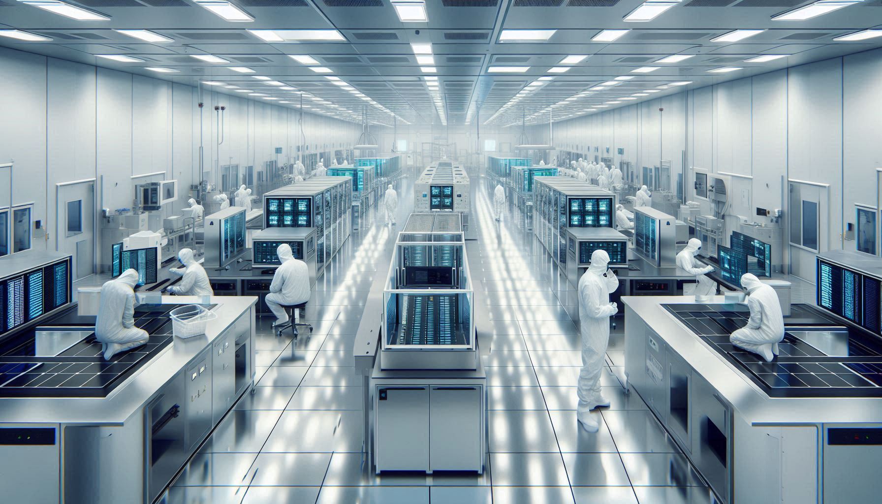
Semiconductor Cleanroom: How to Design HVAC Systems

Advanced semiconductor cleanroom with integrated HVAC system and cleanroom air filtration

Semiconductor fabrication demands ultra‐clean environments to protect delicate wafers and complex integrated circuits. In today’s high‐tech manufacturing, advanced HVAC systems ensure that semiconductor cleanroom maintain optimal temperature, humidity, and air purity. This article explains what a cleanroom is for semiconductor manufacturing, why semiconductors need a cleanroom, how cleanrooms and semiconductor cleaning processes work, and details HVAC design principles, from air filtration to complying with stringent HVAC standards for semiconductor facilities.

What Is a Cleanroom in Semiconductor Manufacturing?

A semiconductor cleanroom is a highly controlled space where particles, temperature, and humidity are kept to strict limits. These rooms adhere to international standards such as ISO 14644‑1 that classify cleanrooms based on the maximum allowable particles per cubic meter. Cleanrooms usually range from ISO Class 1 (the strictest) up to Class 10 or even Class 100, depending on the application. In semiconductor fabs, the typical cleanroom often operates in ISO Class 5 or lower, ensuring that the wafer surfaces remain pristine throughout photolithography, deposition, and etching processes.

Why Do Semiconductors Need a Cleanroom?

Semiconductor devices are built layer by layer on silicon wafers using photolithography and other processes that are extremely sensitive to contamination. Even a single microscopic particle may cause defects, compromises in yield, or electrical shorts. Consequently, semiconductor cleanrooms protect chips from airborne particles, metal ions, and volatile compounds. In addition, stable temperature and humidity conditions prevent device variability caused by thermal expansion or moisture-induced oxidation. Ultimately, maintaining a contaminant‐free environment leads to higher efficiency, reliability, and improved overall wafer yields.

Also Read | Why Temperature and Humidity Control Is Critical in Cleanrooms

How Do You Clean a Semiconductor?

Cleaning semiconductor components is a multi‐step process designed to remove every trace of contamination without damaging the wafer. Typical cleaning steps include:

  • Preliminary Rinse: Using ultra‐pure deionized (DI) water to remove loose particulate matter.
  • Organic Solvent Cleaning: Immersing or wiping the wafer with solvents (e.g., acetone or isopropyl alcohol) to eliminate grease, photoresists, or polymer residues.
  • Oxide Removal: Employing chemical etches like hydrofluoric acid (HF) dips to strip away native oxides before subsequent processing steps.
  • Megasonic or Ultrasonic Cleaning: Applying high‐frequency sound waves in DI water to dislodge particles that cling to the wafer surface.
  • Final Rinse and Drying: Using spin rinse dryers and controlled atmosphere drying to ensure the wafer is completely dry and free of residual contaminants.

These methods together achieve the cleanliness levels required in semiconductor manufacturing.

Semiconductor Cleanroom Standards and Classifications

Cleanroom standards are critical for ensuring that semiconductor processes are not compromised by contaminants. Manufacturers follow guidelines such as ISO 14644‑1 and SEMI standards to set the allowable limits on particle counts. For example, a semiconductor cleanroom may allow no more than 3,520 particles (0.5 µm or larger) per cubic meter of air. Many facilities provide detailed documentation in the form of cleanroom PDFs that outline classification criteria, operational protocols, and layout designs.

Other important criteria include:

  • Cleanroom PDF Guides and Manuals: These documents provide step-by-step procedures for cleanroom construction, maintenance, and gowning procedures.
  • Classification: Semiconductor cleanroom classifications (e.g., Class 1,000 or ISO Class 5) determine the cleanliness level required for various production stages.
  • Manufacturers and Companies: Leading semiconductor cleanroom manufacturers and companies supply customized HVAC solutions, specialized filtration systems, and innovative cleanroom construction materials.
  • Jobs and Training: The semiconductor industry offers many job opportunities, including roles such as cleanroom technicians and HVAC engineers, all of whom must follow strict gowning procedures and layout protocols.
  • Environmental Parameters: Critical operating parameters—such as maintaining a stable temperature (usually around 20 °C to 22 °C) and controlled humidity (typically 40% to 60% RH)—continue to play a pivotal role in the overall design.

HVAC Design for Semiconductor Cleanroom

A robust HVAC design is essential for maintaining a cleanroom environment. Designers must integrate multiple subsystems to meet the demanding requirements of semiconductor manufacturing.

1. Semiconductor HVAC and Cleanroom Air Filtration

Engineers use advanced air filtration systems (HEPA and sometimes ULPA filters) to remove contaminants. In these systems:

  • HEPA filters remove at least 99.97% of 0.3 µm particles, preventing airborne contaminants from reaching sensitive wafer surfaces.
  • Cleanroom Air Filtration is key to maintaining air purity. Filtered air flows downwards through ceiling fan filter units in a smooth, vertical pattern to reduce turbulence.

2. HVAC for Semiconductor: Controlling Temperature and Humidity

Maintaining a controlled environment is key. Semiconductor HVAC systems ensure:

  • Temperature Stability: Semiconductor operations often require temperature control within a narrow range—typically between 20 °C and 22 °C—to avoid process variations due to thermal expansion.
  • Humidity Regulation: Relative humidity is maintained around 40% to 60% to mitigate electrostatic discharge (ESD) issues and prevent moisture condensation on sensitive surfaces.
  • Airflow Management: Unidirectional (laminar) airflow is employed to maintain uniform air distribution and ensure contaminants are efficiently exhausted.

3. Adhering to HVAC Standards for Semiconductor

HVAC standards for semiconductor applications require full compliance with both international and industry-specific guidelines. These include:

  • ISO 14644‑1 Compliance: Establishing the particulate limits and environmental parameters based on the cleanroom classification.
  • SEMI Guidelines: These provide additional criteria for air quality and performance reliability in semiconductor facilities.
  • Energy Efficiency Considerations: While maintaining clean conditions, modern HVAC systems also optimize energy consumption by using variable frequency drives (VFDs) and smart sensors that adjust the system performance in real time.

By incorporating these HVAC standards and using the right combination of filtration, temperature, and airflow controls, semiconductor cleanrooms achieve consistent, high-quality performance.

Semiconductor Cleanroom Design and Construction

Attention to detail in cleanroom design is vital for semiconductor fabrication. Key design considerations include:

  • Layout and Modular Construction: Cleanroom layout must optimize space while ensuring an uninterrupted flow of filtered air. Modular wall panels, raised floors, and dedicated gowning areas facilitate efficient operation and future expansion.
  • Gowning Procedures and Cleanroom Suits: Personnel must wear cleanroom suits (often called “bunny suits”) along with gloves, masks, and shoe covers. Strict gowning procedures reduce particle shedding and protect the clean environment.
  • Cleanroom Construction: Specialized materials—such as non-shedding wall panels and static-dissipative flooring—minimize the generation of particulates. Construction guidelines also incorporate electrical, plumbing, and HVAC system integration.
  • Cleanroom Layout: An effective layout considers pedestrian flow, equipment access, and air return systems, which together contribute to the overall cleanliness of the environment.

Temperature, Humidity, and Environmental Control

Environmental control remains a cornerstone of cleanroom operation. In semiconductor cleanrooms:

  • Temperature is closely managed (typically within ±0.1 °C) to prevent thermal expansion or contraction that could impair chip production.
  • Humidity levels are carefully set between 40% and 60% RH to reduce static electricity and deter condensation.
  • Air Pressure is managed to ensure a positive pressure differential, which blocks contaminants from entering the cleanroom.

These parameters directly influence product yield, making precise HVAC design imperative.

Semiconductor Cleanroom Jobs and Industry Opportunities

The semiconductor industry is expanding rapidly, opening up numerous career paths in cleanroom management and HVAC design. Jobs in this field include:

  • Semiconductor Cleanroom Technicians: Responsible for maintaining cleanliness standards and ensuring strict adherence to gowning procedures.
  • HVAC Engineers: Specialize in designing and optimizing HVAC systems tailored to the stringent requirements of semiconductor fabs.
  • Facility Managers: Oversee cleanroom operations, coordinate maintenance schedules, and ensure compliance with regulatory standards.

Companies investing in semiconductor cleanroom construction and HVAC integration often provide ongoing training, competitive salaries, and opportunities for professional growth.

Conclusion

Semiconductor cleanrooms and their corresponding HVAC systems are critical to producing high‐quality microelectronic devices. By employing advanced cleanroom air filtration, precise temperature and humidity controls, and strictly adhering to HVAC standards for semiconductor environments, manufacturers can ensure that even the smallest contaminants are kept at bay. As semiconductor technologies continue to evolve, the need for optimized HVAC systems grows, driving innovations in cleanroom design, construction, and operational procedures.

If you’re looking to learn more about semiconductor cleanroom standards, layout design, or how to implement robust HVAC for semiconductor applications, many resources—ranging from detailed PDFs to industry webinars—are available to guide you.

FAQs

What is a cleanroom in semiconductor manufacturing?

A semiconductor cleanroom is a controlled environment designed to minimize airborne particles and maintain strict temperature and humidity conditions, ensuring that sensitive wafer fabrication processes remain free from contamination.

Why do semiconductors need a cleanroom?

Semiconductors require cleanrooms because even microscopic contamination can cause defects during photolithography and etching. These environments prevent particle-induced failures and protect the integrity of semiconductor chips.

How do you clean a semiconductor?

Cleaning involves multiple steps: preliminary DI water rinse, solvent washing to remove organics, chemical etching for oxide removal, megasonic or ultrasonic cleaning to dislodge particles, followed by a final rinse and drying.

Which standards govern semiconductor cleanroom?

Cleanrooms follow ISO 14644‑1 classifications and industry‐specific guidelines such as SEMI standards. These ensure that particle counts, temperature, humidity, and airflow are maintained at precise levels.

What role do HVAC systems play in semiconductor cleanroom?

HVAC systems control air filtration, temperature, humidity, and pressure. They maintain a laminar airflow using HEPA or ULPA filters and optimize the environment to comply with strict semiconductor HVAC standards.

How is a semiconductor cleanroom constructed?

Construction involves using modular panels, raised floors, and non‐shed materials, along with dedicated gowning areas and a well-integrated HVAC system. Effective layouts and strict gowning procedures further ensure a contaminant-free environment.

Disclaimer

The content here is intended solely for educational and informational purposes. All case studies, examples, and hypothetical scenarios are illustrative in nature and do not refer to, endorse, or represent any actual company, organization, or product. Any similarity to real-world entities or events is purely coincidental. Readers should verify technical details with independent research before implementation. The author and publisher assume no responsibility for any errors, omissions, or outcomes resulting from this material.

About the Author

Mr. Om Prakash, with over 18 years of hands-on experience in the HVAC industry, brings unmatched expertise in cleanroom, semiconductor, pharmaceutical, data center, commercial, and industrial HVAC systems. As the founder of HVAC Technocrat, he specializes in customized HVAC design, energy efficiency audits, retrofit planning, and turnkey consultancy services across India. He simplifies complex HVAC concepts and shares real-world insights that support professionals, facility managers, and decision-makers. For enquiries or project support, call or WhatsApp at +91 9908091942, email hvactechnocrats@gmail.com, or visit www.hvactechnocrat.com. Also, follow his LinkedIn profile at https://www.linkedin.com/in/hvactechnocrats/.

Innovative HVAC for Semiconductor Manufacturing

A modern semiconductor cleanroom with advanced HVAC systems

The semiconductor industry relies heavily on precision and cleanliness, making HVAC for semiconductor manufacturing a cornerstone of success. These systems ensure that cleanroom environments meet stringent standards like ISO Class 5 or better, which are critical for producing high-quality microchips. Semiconductor fabrication is highly sensitive to environmental conditions, and even minor fluctuations in temperature, humidity, or particle levels can lead to costly defects. In this article, we’ll explore the innovative technologies driving HVAC for semiconductor facilities, address common challenges, and highlight best practices to optimize performance.

Why HVAC is Crucial for Semiconductor Manufacturing

Semiconductor manufacturing involves processes that demand precise control over environmental variables. For instance, photolithography—a technique used to etch circuit patterns onto silicon wafers—requires humidity levels to remain within ±2% to prevent photoresist materials from degrading. Similarly, controlling airborne particles is essential during wafer processing to avoid contamination. This is where HVAC for semiconductor facilities plays a pivotal role, maintaining consistent temperature, humidity, and pressure levels while filtering out submicron particles. To learn more about cleanroom classifications, refer to our detailed guide on ISO Class 5 cleanrooms.

Additionally, advanced HVAC systems contribute to energy efficiency, reducing operational costs without compromising performance. Transitioning to smart controls and AI-driven solutions has become increasingly common in modern facilities.

Emerging Technologies in HVAC for Semiconductor Facilities

As the semiconductor industry evolves, so do the technologies supporting it. Here are some innovations reshaping HVAC for semiconductor manufacturing:

AI-Driven Optimization

Artificial intelligence (AI) is transforming HVAC operations by enabling predictive maintenance and real-time monitoring. For example, AI-powered systems can analyze data from sensors to detect anomalies in airflow or temperature, allowing engineers to address issues proactively. A semiconductor plant in Bengaluru implemented such a system, achieving a 20% reduction in energy consumption while enhancing cleanroom stability. Explore how AI optimizes chiller plants in data centers here.

Desiccant Dehumidification

Controlling humidity is particularly challenging in tropical climates like India’s. Desiccant wheels, which absorb moisture from the air, are increasingly integrated into HVAC systems for semiconductor facilities. This technology ensures low relative humidity levels, even in humid conditions, preventing condensation on sensitive equipment. Discover more about desiccant wheels here.

Energy Recovery Systems

Energy recovery ventilators (ERVs) are gaining traction in semiconductor manufacturing due to their ability to reduce energy costs. ERVs transfer heat and moisture between incoming and outgoing air streams, minimizing the load on HVAC systems. For example, a facility in Hyderabad reduced its HVAC-related energy bills by 15% after installing an ERV system.

Challenges in HVAC for Semiconductor Facilities

Designing HVAC systems for semiconductor manufacturing presents unique challenges. However, addressing these challenges ensures optimal performance and reliability.

Stringent Cleanroom Requirements

Maintaining ISO Class 5 or better standards demands superior filtration systems, such as HEPA and ULPA filters, to trap submicron particles. Additionally, achieving high Air Changes Per Hour (ACPH), often exceeding 600, is essential to maintain ultra-low particle counts. Learn how high ACPH impacts cleanroom performance here.

High Energy Consumption

Semiconductor cleanrooms consume up to 50 times more energy than conventional office spaces, primarily due to continuous operation and strict environmental controls. To mitigate this, facilities are adopting energy-efficient technologies like geothermal cooling and solar-powered HVAC systems.

Scalability

As production scales, HVAC systems must adapt without compromising performance or efficiency. Modular designs allow for easy expansion and customization, ensuring long-term flexibility.

Sustainability in HVAC for Semiconductor Manufacturing

Sustainability is becoming a priority in the semiconductor industry, driven by global initiatives like IGBC and LEED certifications. Here’s how HVAC systems contribute to sustainable practices:

Geothermal Cooling

Some facilities are adopting geothermal HVAC systems, which use the earth’s natural thermal properties to cool cleanrooms efficiently. Explore geothermal options here.

Solar-Powered HVAC

Integrating solar panels with HVAC systems reduces reliance on grid electricity. A semiconductor plant in Gujarat achieved a 25% reduction in operational costs using solar-powered units.

Smart Controls

IoT-enabled thermostats and sensors optimize energy usage by adjusting settings based on occupancy and production schedules. This not only reduces energy consumption but also enhances system reliability.

Case Studies: Real-World Applications

To better understand the impact of innovative HVAC systems, consider these examples:

Precision Airflow Management

A semiconductor fab in Taiwan implemented a hot aisle/cold aisle configuration, improving cooling efficiency by 30%. This setup ensures consistent airflow across server racks and process tools.

Particle-Free Environments

A cleanroom in Chennai achieved ISO Class 3 certification by integrating advanced filtration systems and pressure differential controls. Learn why pressure differentials are crucial here.

Best Practices for HVAC in Semiconductor Facilities

To maximize the efficiency of HVAC for semiconductor manufacturing, consider the following best practices:

  • Regular maintenance schedules help ensure filters, ducts, and compressors function optimally.
  • Airflow simulation using computational fluid dynamics (CFD) analysis helps identify potential hotspots or contamination risks.
  • Redundancy planning incorporates backup systems to maintain uninterrupted operation during HVAC failures.

For insights into effective maintenance strategies, check out our guide on AC service near me.

FAQs: HVAC for Semiconductor Manufacturing

What is the role of HVAC in semiconductor manufacturing?

HVAC systems regulate temperature, humidity, and particle levels in cleanrooms, ensuring optimal conditions for chip fabrication.

How does AI improve HVAC efficiency in semiconductor facilities?

AI enables predictive maintenance and real-time monitoring, reducing energy consumption and preventing costly downtime.

What are the challenges in designing HVAC for semiconductor cleanrooms?

Key challenges include meeting stringent cleanliness standards, managing high energy consumption, and ensuring scalability.

What technologies enhance energy efficiency in semiconductor HVAC systems?

Technologies like desiccant dehumidifiers, energy recovery ventilators, and geothermal cooling contribute to energy savings.

How important is sustainability in semiconductor HVAC design?

Sustainability reduces operational costs and aligns with global green building initiatives, making it a growing focus for manufacturers.

Where can I learn more about cleanroom HVAC standards?

Explore resources like the ISO Class 5 cleanroom guide for detailed insights.

Disclaimer

Some links in this article are affiliate links, such as those for Amazon products. These may generate a small commission at no extra cost to you, supporting our work. We never compromise editorial integrity for partnerships.

About the Author

Mr. Om Prakash, with over 18 years of hands-on experience in the HVAC industry, brings unmatched expertise in cleanroom, pharmaceutical, semiconductor, data center, commercial, and industrial HVAC systems. As the founder of HVAC Technocrat, he specializes in customized HVAC design, energy efficiency audits, retrofit planning, and turnkey consultancy services across India. His deep understanding of critical environments and complex building needs ensures every solution is efficient, reliable, and future-ready. Through his writings, he simplifies HVAC concepts and shares real-world insights to support professionals, facility managers, and decision-makers. For any enquiries or project support, feel free to call or WhatsApp at +91 9908091942, email at hvactechnocrats@gmail.com, or visit www.hvactechnocrat.com.